Topic guide · Chips and light
How does EUV light print a chip?
By projecting a chip’s pattern with light so short that air would swallow it. A laser hits a speeding drop of tin twice, once to flatten it and once to turn it into a plasma hotter than the surface of the Sun, and the plasma glows at 13.5 nm. ASML’s machines do this 50,000 times a second. Air and glass absorb that light, so everything runs in a vacuum and mirrors take the place of lenses; after 11 reflections only about 2% of the light reaches the wafer. That is enough to print a chip’s finest details, about 13 nm across, or 8 nm in ASML’s newest High-NA machines.
- Wavelength
- 13.5 nm
- Tin drops hit
- 50,000 a second
- Light left after 11 reflections
- ≈ 2%
- Smallest detail
- 13 nm · High-NA 8 nm
Published figures · ASML, Trumpf, Wikipedia Each mirror keeps about 70%, and 0.7¹¹ ≈ 2%. Smallest detail = k1 × λ ÷ NA, so 0.32 × 13.5 nm ÷ 0.33 ≈ 13 nm.
Video · by Konstantin Saifoulline
How chipmaking uses extreme ultraviolet light
His browser model of an EUV scanner: tin droplets hit twice, the plasma flash, eleven mirrors and the wafer. The page has his recording, our film about it and a link to the model itself.
Model · a teaching model, not ASML data
Why does a shorter wavelength print smaller?
A chip machine is a projector that shrinks. A mask holds the pattern for one layer of a chip, and the optics project it four times smaller onto a silicon wafer. The finest detail it can print is set mostly by the light.
ASML writes the limit as the Rayleigh criterion: CD = k1 · λ / NA. CD, the critical dimension, is the smallest feature. λ is the wavelength. NA, the numerical aperture, is how much light the optics can collect. k1 covers everything else in the process, and ASML puts its physical limit at 0.25.
Why the wavelength? Light spreads as it passes the edges of a tiny pattern, and the lens catches only part of that spread. Resolution is limited by the wavelength and by how much of the diffracted light the lens captures. So a shorter wavelength, or optics with a larger NA, prints finer patterns.
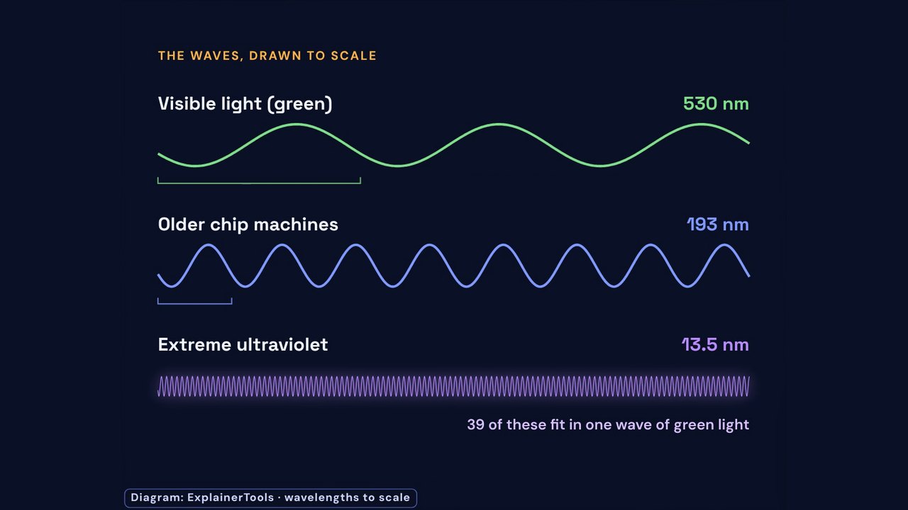
The numbers show what EUV buys. The best deep-ultraviolet machines use 193 nm light with an NA of 1.35 and print about 38 nm in one exposure, Wikipedia’s comparison shows. EUV light is 13.5 nm, about 14 times shorter. With an NA of only 0.33, it prints about 13 nm. The picture at the top draws three waves to scale: 39 EUV waves fit in one wave of green light.
How does the machine make 13.5 nm light?
With a laser and a stream of tin. Trumpf, which builds the laser, describes the source: a generator fires 50,000 droplets of tin a second through a vacuum chamber, and a CO₂ laser with more than 30 kilowatts of average power hits every droplet twice. ASML says the molten drops fly at 70 meters a second.
Why twice? A droplet is smaller than the laser’s focus spot, so a single hit could not pass on the pulse’s full power. A weak pre-pulse comes first and spreads the tin out; ASML says it flattens each drop into a pancake. The main pulse follows close behind and strikes with full power. The tin becomes a plasma hotter than the surface of the Sun.
That plasma is the light source. Tin ions missing 8 to 13 electrons give off light in peaks around 13.5 nm, while neutral atoms and solid matter cannot emit EUV at all. A collector mirror gathers the light and sends it on into the machine.
Why mirrors and a vacuum?
Because almost everything absorbs EUV light. ASML says it is absorbed even by air, so the whole light path, from source to wafer, sits in high vacuum. Glass absorbs it too, so there are no lenses. Every optic in the machine is a mirror, and so is the mask.
They are not ordinary mirrors. Each is a stack of alternating layers of molybdenum and silicon, and the small reflections from the many layers add up through interference. Each mirror still absorbs around 30% of the light that hits it, Wikipedia notes. After the collector, the beam meets four mirrors in the illuminator, then the mask, then six mirrors in the projection optics. With 11 reflections, only about 2% of the source light reaches the wafer: 0.7 multiplied by itself 11 times is about 0.02.
The mirrors also have to be almost perfect. Zeiss, which makes them, says that scaled up to the size of Germany, the largest unevenness on one of its EUV mirrors would be a tenth of a millimeter.
What does the light do on the wafer?
It prints one layer of a chip. The wafer is first coated with photoresist, a film that reacts to light. The mirrors project the mask’s pattern onto it, shrunk four times, one field at a time; on most EUV machines a field is 26 × 33 mm. ASML’s wafer stage places the wafer to within a quarter of a nanometer for each exposure.
Where the light lands, the resist changes. In the most common kind, positive resist, the exposed parts become soluble in a developer and wash away. The resist that is left protects the wafer while an etch removes material from the open areas. That is one layer’s pattern. A wafer may go through the cycle as many as 50 times, one layer after another.
At these sizes, chance starts to matter. EUV printing is particularly sensitive to random, or stochastic, defects, and Wikipedia notes that the odds of a failure rise steeply as features shrink.
What does High-NA change, and what comes next?
High-NA works on the bottom of the formula. A larger NA means optics that collect more light, and a smaller CD. ASML’s High-NA machines raise the NA from 0.33 to 0.55, and their resolution goes from 13 nm to 8 nm, Wikipedia’s comparison lists.
When ASML showed the machine in February 2024, Reuters reported that it costs about $350 million and is the size of a double-decker bus. Its larger mirrors are made by Carl Zeiss. ASML said it lets chipmakers shrink the smallest features by up to 40% and nearly triple the density of transistors. The bigger optics have a cost: they shrink the pattern 4× one way and 8× the other, so each field is 26 × 16.5 mm, half the area of before.
The next step is more light. In February 2026, ASML told Reuters its researchers had found a way to raise the source to 1,000 watts, from 600 watts now. They double the tin drops to about 100,000 a second and shape each with two smaller laser bursts instead of one. That should let customers process about 330 wafers an hour on each machine by the end of the decade, up from 220 now.
Try it: hit the tin, follow the light, widen the optics
- 1 See
Open his EUV machine. Under Follow, tap Tin, then set Time to Slow-mo. It runs 40 times slower, so you can watch each droplet hit twice: a weak pre-pulse flattens it, then the main pulse turns it into plasma.
- 2 Change
Tap Light and follow the beam from the plasma through eleven mirrors to the wafer. Reaches the wafer reads 1.4%, because in his model each mirror reflects about 68%.
- 3 Understand
Tap All, then switch Optics from 0.33 NA to High-NA. Smallest line falls from 12.3 nm to 7.4 nm: the Rayleigh criterion with a larger NA. Throughput falls too, because his model gives High-NA a little less light at the wafer and more time stepping between its smaller fields.
His model runs in the browser and works best on a larger screen. Split cuts the machine in half and Exploded pulls every module apart. Its numbers are his model’s, and the next section says where they differ from the companies’.
Where does his model stop?
His notes say it plainly. It is “a generic EUV scanner, not a specific product,” built from public figures, and his post on X adds: “It is a model, not ASML data.” The droplets, the plasma and the beam are drawn much larger than real, and the internal layout is simplified.
Some of his numbers differ from the companies’. His plasma is about 220,000 K; ASML’s page says about 500,000 K. His mirrors reflect about 68% each and leave 1.4% of the light at the wafer, where Wikipedia’s round 70% leaves about 2%. His throughput comes from what his notes call “our model”: about 160 wafers an hour from a 250 W source, while ASML’s machines run at about 600 W and 220 wafers an hour, Reuters reported in February 2026. His October 13 post, and the video the film excerpts, give other figures again: eleven mirrors that each keep 71%, and one photon in 148 reaching the wafer.
So read his model for the path the light takes and why every step costs light, not for a real machine’s numbers. The film uses short excerpts of his video and of ASML’s own footage, credited on screen. Its narration takes its figures from ASML, Trumpf and Wikipedia, not from his panels.
Explore by question
One machine, and the questions around it: how its light is made, why the light has to be so short, why tin glows at one wavelength, and what the light ends up printing.
His EUV machine
Konstantin Saifoulline’s model · not ASML data
- VideoHow chipmaking uses extreme ultraviolet lightHis recording of the model: tin droplets hit twice, the plasma flash and the light’s path through eleven mirrors. The page also has our 45-second film and a link to the model itself.by Konstantin Saifoulline
Why short light prints small
Waves spread out after they pass a narrow gap. That spreading, diffraction, is why the wavelength limits how small a pattern can be printed.
- Interactive demoRipple TankChoose a slit setup from the Example menu and watch the waves fan out past the gap.by Paul Falstad · Opens on the creator’s site
Why tin glows at one wavelength
A gentler version of the tin plasma: excited atoms give off light at wavelengths set by the atom. Tin ions glow near 13.5 nm; oxygen high in the sky glows green at 557.7 nm.
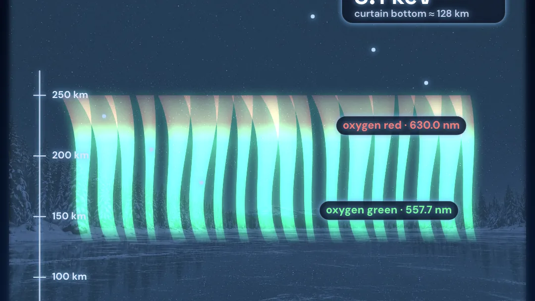 Interactive · Aurora ChamberWhy are the northern lights green?Raise the incoming electrons’ energy and watch oxygen’s green and red and nitrogen’s purple stack by height.
What the light prints
Each exposure prints part of one layer of a chip. This video zooms down to the transistors those layers make.
- VideoZooming Into a CPUZoom from a processor package down to its transistors, the parts lithography patterns layer by layer.by Branch Education
Common questions
Why not use visible or deep-ultraviolet light?
Their waves are too long for a chip’s finest details. Ultraviolet means beyond violet, the shortest visible color, and even the best deep-ultraviolet machines, at 193 nm, print only down to about 38 nm in one exposure. To go finer, chipmakers expose the same layer several times, which is called multiple patterning; TSMC’s 7 nm process used it extensively. EUV, at 13.5 nm, prints about 13 nm in one pass.
Why tin?
Because hot tin ions glow strongly at the right wavelength. Wikipedia notes that tin ions missing 8 to 13 electrons give emission peaks around 13.5 nm, and at 13.5 nm molybdenum and silicon mirrors can in theory reflect about 75%. Neutral atoms and solid tin cannot emit EUV, which is why each droplet has to become a plasma first.
How much does an EUV machine cost?
A typical EUV machine weighs nearly 200 tons and costs around $180 million, Wikipedia notes. ASML’s High-NA machine costs about $350 million, Reuters reported in February 2024. ASML then had 10 to 20 orders for it and was building capacity to deliver 20 a year by 2028.
Why does only ASML make them?
Because it took decades and a whole alliance. Zeiss, which makes the mirrors, wrote in 2021 that the foundations were laid about 25 years earlier. Trumpf makes the laser, ASML builds the system, and ASML works with around 1,200 partners. In the late 2010s it became the first and only company to market an EUV tool, Reuters reported. Nikon and Canon of Japan make lithography machines too, but for older generations of chips.
What does High-NA mean?
High numerical aperture. NA measures how much light the optics can collect, and a larger NA prints smaller features. ASML’s High-NA machines raise it from 0.33 to 0.55, taking resolution from 13 nm to 8 nm. The trade is a smaller exposure field: 26 × 16.5 mm instead of 26 × 33 mm.
Concepts in this guide
Each one has a plain one-line definition in Concepts A–Z, with every model, film and post where it comes up.
Sources and credits
- Konstantin Saifoulline · EUV chip machine, airsup lab His browser model and its notes, read October 31, 2026: the Follow, Optics, Time and Machine controls, the readouts, and his figures (about 220,000 K, 68% a mirror, 1.4% at the wafer, 12.3 and 7.4 nm, about 160 wafers an hour). His post on X of October 13, 2026, carries the video the film excerpts and says “It is a model, not ASML data.”
- ASML · The hottest thing about ASML machines Two laser pulses per tin drop, 50,000 times a second, drops at 70 m/s; a plasma of about 500,000 K; the whole light path in high vacuum; multilayer mirrors instead of lenses; the pattern shrunk 4×; the wafer placed to a quarter of a nanometer.
- Trumpf · Flashes of light in a vacuum The laser maker on the pre-pulse and main pulse, 50,000 tin droplets a second, more than 30 kW of CO₂ laser power, the collector, and why a droplet smaller than the focus spot needs two hits.
- ASML · The Rayleigh criterion for resolution CD = k1 · λ / NA, what each term means, and the physical limit of k1 = 0.25.
- Wikipedia · Photolithography Resolution limited by the wavelength and by the diffracted light the lens captures; positive resist, developing and etching; up to 50 lithography cycles per wafer.
- Wikipedia · Extreme ultraviolet lithography Absorption by air and glass; about 30% lost per mirror and about 2% left after 11 reflections; 13 nm at NA 0.33, 8 nm at 0.55 and 38 nm for 193 nm immersion; tin ions’ emission near 13.5 nm; field sizes; the $180 million price; stochastic effects; TSMC’s 7 nm multi-patterning.
- ZEISS SMT · EUV lithography: a European joint project October 20, 2021. Zeiss makes the mirrors, Trumpf the laser and ASML the system; about 25 years of work; around 1,200 partners; mirror flatness scaled to the size of Germany.
- Reuters · ASML’s next chip challenge: rollout of its new $350 million “High NA EUV” machine February 9, 2024, via Yahoo Finance. The price and bus-sized machine, Zeiss mirrors, features up to 40% smaller and nearly triple the transistor density, 10 to 20 orders, and ASML as the only maker of EUV tools.
- Reuters · ASML unveils EUV light source advance that could yield 50% more chips by 2030 February 23, 2026. A 1,000 W source against 600 W now, about 100,000 tin drops a second shaped by two bursts, and about 330 wafers an hour per machine by 2030, up from 220.
Every creator named here made the work we link to. Listing it does not imply a partnership or endorsement.